|
|
| |
|
 | Search: |
|
|
 |

|
|
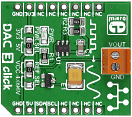
DAC3 click carries Microchip's MCP4726 IC, a 12-bit digital-to-analog converter, along with voltage output screw terminals. The digital value is converted to the appropriate voltage level in the range between GND and REFERENCE (VCC or 4.096V), which is proportional to the received 12-bit number. MCP4726 also integrates EEPROM for storing DAC register and configuration bit values. The board communicates with the target board MCU through the mikroBUS I2C interface (SCL, SDA pins). Standard (100 kHz), fast (400 kHz) and highspeed (3.4 MHz) I2C modes are available. Uses either a 3.3V or a 5V power supply. |
|
|
|
|
 |

|
|
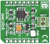
The DAC Click board is an accessory board in mikroBus form factor. It includes the MCP4921 12-bit Digital-to-Analog Converter which features a SPI interface and optional dual-buffered output. The board provides high accuracy and low noise performance for industrial applications where calibration or compensation of signals, such as temperature, pressure and humidity, are required. The board is set to use the 3.3V mikroBus power supply by default, however soldering the PWR SEL SMD jumper to the 5V position will allow it to be used with 5V mikroBus systems. |
|
|
|
 |

|
|
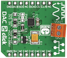
DAC2 click carries LTC2601CDD, a 16-bit digital-to-analog converter, along with voltage output screw terminals. The chip has high rail-to-rail output drives (±15mA, Min) and double-buffered data latches. The click board communicates with the target MCU through the mikroBUS SPI interface with clock rates up to 50MHz. Additionally, the CLR pin, in place of default mikroBUS RST pin, clears all the registers. The board uses either a 3.3V or 5V power supply. You can also set the reference voltage either to VCC or 4.096V. |
|
|
|
 |

|
|
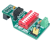
The DAC Board is an accessory board provided with a D/A converter MCP4921 with a serial peripheral interface (SPI). This board is ideal for connecting microcontrollers with analog devices. |
|
|
|
 |

|
|
VREG click is a digitally controlled DC Voltage regulator in mikroBUS™ form factor. The design is based on the well-known LM317 circuit, with the addition of a 12-bit DAC, 12-bit ADC, and an Operational Amplifier. Two pairs of screw terminals serve as inputs and outputs.
The LM317 IC is a reliable regulator with typical line regulation of 0.01% and load regulation of 0.1%. It also has internal short-circuit current limiting and thermal overload protection.
The circuit regulates voltage by turning all input/output difference into heat (effectively dissipating all the excess power). If it gets too hot it may damage the board or cause unexpected behaviour.
Because of that, the board’s operating range is defined by two factors. 1) maximum input voltage and current (should not exceed 20V/1A); and 2) maximum wattage arising from current and I/O voltage difference (should not exceed 2W, measured as I x (Input V - Output V).
The board also carries a MOSFET chip to toggle the output on and off.
VREG click communicates with the target board MCU through the SPI interface (CS, SCK, MISO, MOSI). The board can use either a 3.3V or a 5V power supply.
It is also possible to use the board’s power supply as the Input, by resoldering the onboard INPUT SEL jumper. |
|
|
|
 |
|
|

