Audio Amp 2 click is a highly efficient class D audio amplifier, using the TDA7491, a dual BTL class-D audio amplifier IC, capable of delivering up to 20W to 8? load. This amplifier IC features high-efficiency output stage drivers and clever design, allowing it to deliver a reasonably high power to the connected speakers, using only GND polygon on the PCB for heat dissipation. In the BTL topology, the output DC blocking capacitors are not required. This allows for simpler design and lower power losses, especially with no input signal. The TDA7491 amplifier IC is equipped with a set of protection features, that allow reliable operation.
Besides the protection features that include short-circuiting protection and thermal overload protection, this Click board™ features a few more options that ensure flawless operation of this amplifier Click board™. Features such as the dedicated diagnostic pin, reduced pop sound on Power ON/OFF, mute and standby options, four selectable input gain settings, low noise, and THD, allow a pleasant experience when using the Audio Amp 2 click. This amplifier Click board™ can be used wherever a quality audio amplification is required.
How does it work?
The main active component of this Click board™ is the TDA7491, a 20W dual BTL class-D audio amplifier IC, from STMicroelectronics. This IC uses the bridge tied load (BTL) topology, which means that the output load is driven by two amplifier stages, one of them being inverted. This results in twice the voltage swing on the output, or four times more power. This also means higher power dissipation, but due to the high efficiency of the TDA7491, the power dissipation is still low enough to be handled by an exposed IC pad.
This amplifier offers a low noise and good quality audio amplification. The frequency response of the amplifier goes from under 20Hz to above 20kHz, covering the entire audio range of the spectrum. Total Harmonic Distortion (THD) 10% at maximum output power, with the 8? load. However, THD decays rapidly as the output power reduces, and power supply voltage rises, respecting the maximum ratings of this IC. The datasheet of the TDA7491 IC offers detailed information about technical characteristics of the amplifier IC itself.
The output modulation scheme of the BTL is the unipolar pulse width modulation (PWM). The output voltage varies between 0V and +VCC for the positive output driver and between 0V and -VCC for the negative output driver. For 0V at the input, the outputs theoretically cancel out each other, resulting with no DC component at the output. In practice, a small delay is introduced, to avoid both stages switching simultaneously, when the input is 0V. Using unipolar PWM scheme simplifies
The power amplifier IC has a protection against the pop sounds when powering the device ON or OFF. However, standby and mute pins provide a way to further reduce the startup noises. STBY pin of the IC puts the device in the Standby mode. This will turn the internal power demanding circuitry OFF, reducing the power consumption to a minimum. MUTE pin allows the inputs to be rerouted internally to GND. By combining STBY and MUTE modes, it is possible to completely avoid pop sounds at the power up or shut down. STBY pin is routed to the mikroBUS™ CS pin and it is labeled as STB, while the MUTE pin is routed to the mikroBUS™ PWM pin, labeled as MUTE.
This Click board™ allows selection of the input gain. Input signal gain staging is important in order to provide the most adequate input level for the amplifier IC. For example, if the input signal is too low, the amplifier might not be able to reach the required output power. Therefore, a corrective gain is applied to the input signal. This is done by applying logic levels to two GAIN pins of the TDA7491 IC (GAIN0 and GAIN1). The truth table below describes how to set the logic levels of these pins to achieve the required signal gain. GAIN0 pin is routed to the mikroBUS™ AN pin, while the GAIN1 pin is routed to the mikroBUS™ RST pin. Pins are labeled as GN0 and GN1 respectively.
DIAG pin allows monitoring of the fault conditions. When the short-circuit or thermal overload protection is activated, the DIAG pin will be set to a HIGH logic level by means of the onboard pull-up resistor, signaling the fault condition to the host MCU. This is an open drain output, which actively sinks current when no fault condition exists, keeping this pin to a LOW logic state. This pin is routed to the mikroBUS™ INT pin, labeled as DIA.
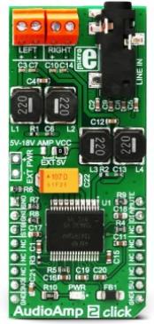
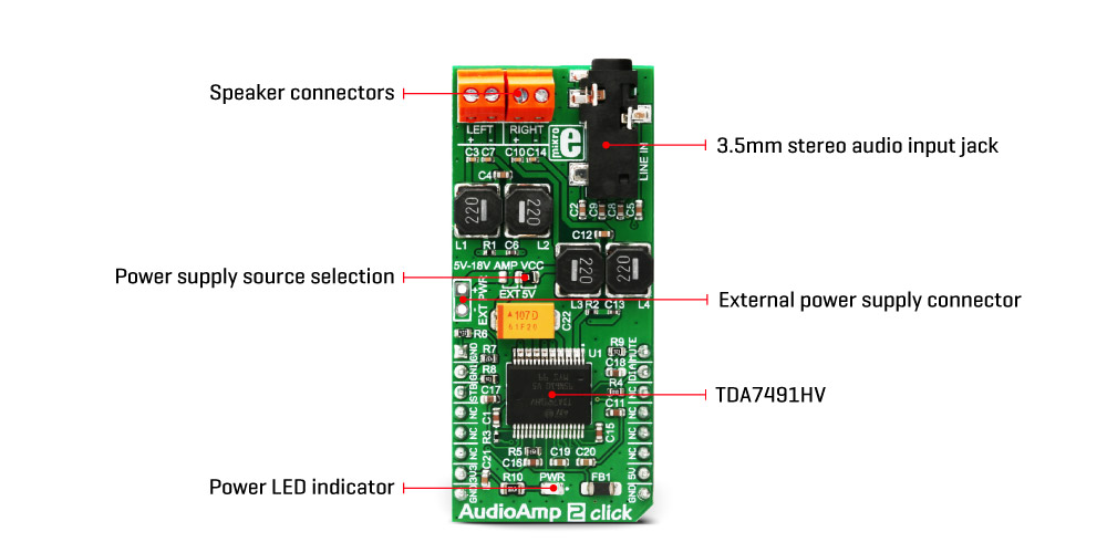
The Click board™ is equipped with 3.5mm stereo jack connector, used to connect the line level audio input. Besides the input jack, there are also two screw terminals, used for connecting the output speakers (4? to 8?).
By default, the Click board™ is powered via the mikroBUS™ 5V rail. This will allow the amplifier to work with limited power. Therefore, an external header is provided, which allows the external power supply to be used, with up to 18V. To select the external power supply, a SMD jumper labeled as AMP VCC needs to be placed to the EXT position.
Specifications
Type
Audio
Key Features
High output power with low dissipation, requiring no heat sinks, low THD and SNR, integrated short circuit detection, undervoltage, and overtemperature protection
Interface
GPIO
Input Voltage
3.3V,5V
Click board size
L (57.15 x 25.4 mm)
Pinout diagram
This table shows how the pinout on AudioAmp 2 click corresponds to the pinout on the mikroBUS™ socket (the latter shown in the two middle columns).
Notes
Pin
Pin
Notes
Gain Setup Pin 0
GN0
1
AN
PWM
16
MUTE
Mute Function
Gain Setup Pin 1
GN1
2
RST
INT
15
DIA
Diagnostic Interrupt
Standby Function
STB
3
CS
RX
14
NC
NC
4
SCK
TX
13
NC
NC
5
MISO
SCL
12
NC
NC
6
MOSI
SDA
11
NC
Power supply
3.3V
7
3.3V
5V
10
5V
Power Supply
Ground
GND
8
GND
GND
9
GND
Ground
Truth table
Gain Setup
20dB
26dB
30dB
32dB
GN0
L
L
H
L
GN1
L
H
L
H
On-board jumpers and indicators
Label
Name
Default
Description
LD1
PWR
-
Power LED indicator
AMP VCC
AMP VCC
Right
Power supply source selection: left position external PSU, right position 5V
N1X2
EXT VCC
-
External power supply connector
LINE IN
LINE IN
-
3.5mm stereo audio input jack
LEFT
LEFT
-
Lef speaker connector
RIGHT
RIGHT
-
Right speaker connector
Software support
We provide a library for the AudioAmp 2 Click on our LibStock page, as well as a demo application (example), developed using MikroElektronika compilers. The demo can run on all the main MikroElektronika development boards.
Library Description
Library offers a choice to put the device in desired mode (Standby, Mute or Play Mode) and to select the gain to the desired value (20, 26, 30 or 32dB). For more details check the documentation.
Key functions :
uint8_t audioamp2_setMode( uint8_t selMode ) - The function puts the device in the desired mode.
uint8_t audioamp2_setGain( uint8_t selGain ) - The function performs the gain selection.
uint8_t audioamp2_checkDiagnostic( void )- The function checks are undervoltage, overcurrent or thermal protection activated.
Example description
The application is composed of three sections :
System Initialization - Initializes peripherals and pins. Application Initialization - Initializes GPIO driver and puts the device in Standby Mode as default operation mode and selects 20dB as default gain selection. Application Task - (code snippet) - Activates Mute operation mode for 4 seconds and after that activates Play mode. When the device is in Play mode then changes the gain selection, first sets the minimum gain (20dB) for 8 seconds and then sets the maximum gain (32dB) for 8 seconds too. Note: Internally, the gain is set by changing the feedback resistors of the amplifier.
The full application code, and ready to use projects can be found on our LibStock page.
Other mikroE Libraries used in the example:
UART
Additional notes and information
Depending on the development board you are using, you may need USB UART click, USB UART 2 click or RS232 click to connect to your PC, for development systems with no UART to USB interface available on the board. The terminal available in all MikroElektronika compilers, or any other terminal application of your choice, can be used to read the message.