These features allow HZ to V 2 click to be used in various frequency to voltage applications: in instrumentation, industrial, and automation markets. It is well suited for use in A/D conversion, long-term integration, frequency to voltage conversion, RPM measurement, capacitance measurement, and similar applications which can benefit from an accurate and reliable frequency to voltage conversion. Its function can be complemented by the V to Hz 2 click, which does the opposite type of conversion: DC voltage to frequency. This can be utilized to build an FM modulator/demodulator application, for example.
How does it work?
The main component of Hz to V 2 click is the VFC32KU, a voltage-to-frequency and frequency-to-voltage converter from Texas Instruments. It accepts a signal with the frequency within a range between 200Hz and 120kHz on the input and generates DC voltage with the level corresponding to the input frequency, ranging from 0V to 10V, with a highly linear response. The output DC voltage level is further scaled down by the voltage divider on the VFC32KU output, in order to achieve levels acceptable by the MCU. This makes the DC voltage output suitable for sampling, or further processing by the host MCU.
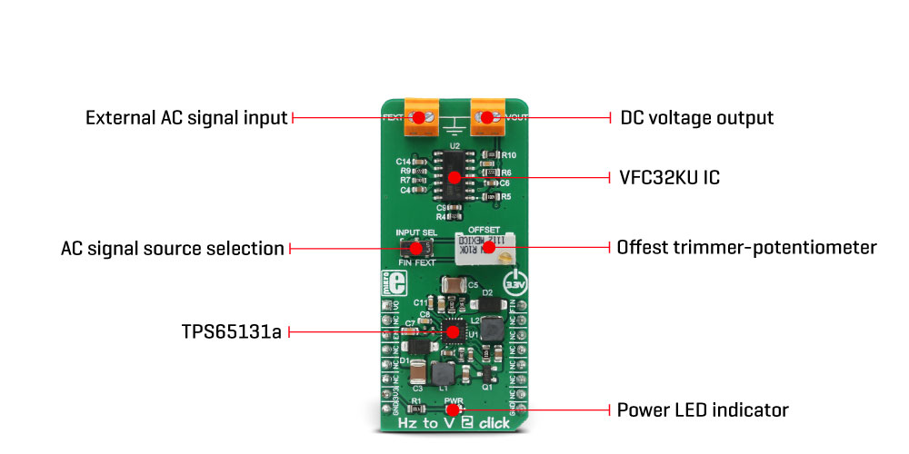
The input signal within the specified frequency range can be applied to either the PWM pin of the mikroBUS™ labeled as FIN on this Click board™ or to the external signal input terminal labeled as FEXT. This signal is AC coupled by a 1nF capacitor, meaning that no DC component will be affecting the connected source. The signal input source can be selected by the onboard switch, labeled as INPUT SEL. A DC voltage output ranging up to 3.3V is available both on the AN pin of the mikroBUS™ labeled as the VO, and the output terminal - labeled as the VOUT on this Click board™.
An onboard high-precision OFFSET potentiometer is used to fine-tune the output of the Click board™. It can be calibrated by using the offset potentiometer, by introducing a signal of a known frequency to either FEXT input terminal or the PWM input pin. An offset trimming procedure should be executed before the first use of the Click board™, since even slight variations in the components tolerances could affect the value at the output. It is recommended to correct the offset after longer time intervals, to compensate for the aging of the passive components on the Click board™.
The VFC32KU IC requires a dual power supply with ±15V. Therefore, this Click board™ utilizes another IC in order to provide the required voltages. It uses the TPS65131, a positive and negative output DC/DC Converter IC, also from Texas Instruments. This DC/DC converter has already been used in Boost-INV 2 click, so it was tested "on the field" for this purpose. Providing well-stabilized output with the plenty of power headroom, it is a perfect solution for the HZ to V 2 click, also.
To enable the conversion circuitry, the EN pin of the TPS65131 boost converter should be pulled to a HIGH logic level. This will activate the boost converter and provide the required power for the VFC32KU IC. This pin is routed to the mikroBUS™ CS pin and it is labeled as EN.
Specifications
| Type |
Measurements |
| Applications |
It can be used in instrumentation, industrial, and automation markets. It is well suited for use in A/D conversion, long-term integration, frequency to voltage conversion, RPM measurement, capacitance measurement, frequency demodulation, and similar applications |
| On-board modules |
VFC32KU, a voltage-to-frequency and frequency-to-voltage converter from Texas Instruments; TPS65131, a positive and negative output DC/DC Converter, from Texas Instruments |
| Key Features |
Hz to V click features very good linearity, covers a wide frequency range and it has good temperature stability. Onboard high-precision trimmer potentiometer for increased accuracy of the converted DC voltage output |
| Interface |
GPIO |
| Input Voltage |
3.3V |
| Click board size |
L (57.15 x 25.4 mm) |
Onboard jumpers and settings
| Label | Name | Default | Description |
|---|
| LD1 |
PWR |
- |
Power LED indicator |
| SW1 |
INPUT SEL |
Left |
Input signal source selection: left position mikroBUS™ FIN pin, right position FEXT input terminal |
| TB1 |
VOUT |
- |
Converted DC voltage output |
| TB2 |
FEXT |
- |
External signal input |
Pinout diagram
This table shows how the pinout on Hz to V 2 click corresponds to the pinout on the mikroBUS™ socket (the latter shown in the two middle columns).
| Notes | Pin |  | Pin | Notes |
|---|
| Voltage OUT |
VO |
1 |
AN |
PWM |
16 |
FIN |
Signal IN |
|
NC |
2 |
RST |
INT |
15 |
NC |
|
| Boost IC Enable |
EN |
3 |
CS |
RX |
14 |
NC |
|
|
NC |
4 |
SCK |
TX |
13 |
NC |
|
|
NC |
5 |
MISO |
SCL |
12 |
NC |
|
|
NC |
6 |
MOSI |
SDA |
11 |
NC |
|
| Power Supply |
3.3V |
7 |
3.3V |
5V |
10 |
NC |
|
| Ground |
GND |
8 |
GND |
GND |
9 |
GND |
Ground |
Software support
We provide a demo application for Hz to V 2 click on our Libstock page, as well as a demo application (example), developed using MikroElektronika compilers. The demo can run on all the main MikroElektronika development boards.
Library Description
Library provides generic functions for working with the click board.
Key functions :
void hztov2_enPin(uint8_t pinState) - Function for enabling the click board.void hztov2_adcInit() - Prepare the ADC for voltage readings.float hztov2_adcRead() - Read the voltages and return the return the float voltage value.
Example description
The application is composed of three sections:
- System Initialization - Initializes GPIO and UART structures.
- Application Initialization - Power on the click board and initializeS the ADC.
- Application Task - Voltage reading is done from the analog pin and the conversion result is converted and output via the UART output.
void applicationTask()
{
 float voltage;
 char txt[20];

 voltage = hztov2_adcRead();
 if(voltage<0.99)
 {
 voltage = voltage * 1000.0;
 FloatToStr(voltage,txt);
 txt[5] = 'm';
 txt[6] = 'V';
 txt[7] = 0;
 }
 else
 {
 FloatToStr(voltage,txt);
 txt[5] = ' ';
 txt[6] = 'V';
 txt[7] = 0;
 }

 mikrobus_logWrite(txt,_LOG_LINE);
 Delay_ms(100);
}
The full application code, and ready to use projects can be found on our LibStock page.
Other mikroE Libraries used in the example:
- UART Library
- Conversions Library
- C_String Library
- ADC Library
Additional notes and information
Depending on the development board you are using, you may need USB UART click, USB UART 2 click or RS232 click to connect to your PC, for development systems with no UART to USB interface available on the board. The terminal available in all MikroElektronika compilers, or any other terminal application of your choice, can be used to read the message.
mikroSDK
This click board is supported with mikroSDK - MikroElektronika Software Development Kit. To ensure proper operation of mikroSDK compliant click board demo applications, mikroSDK should be downloaded from the LibStock and installed for the compiler you are using.
For more information about mikroSDK, visit the official page.